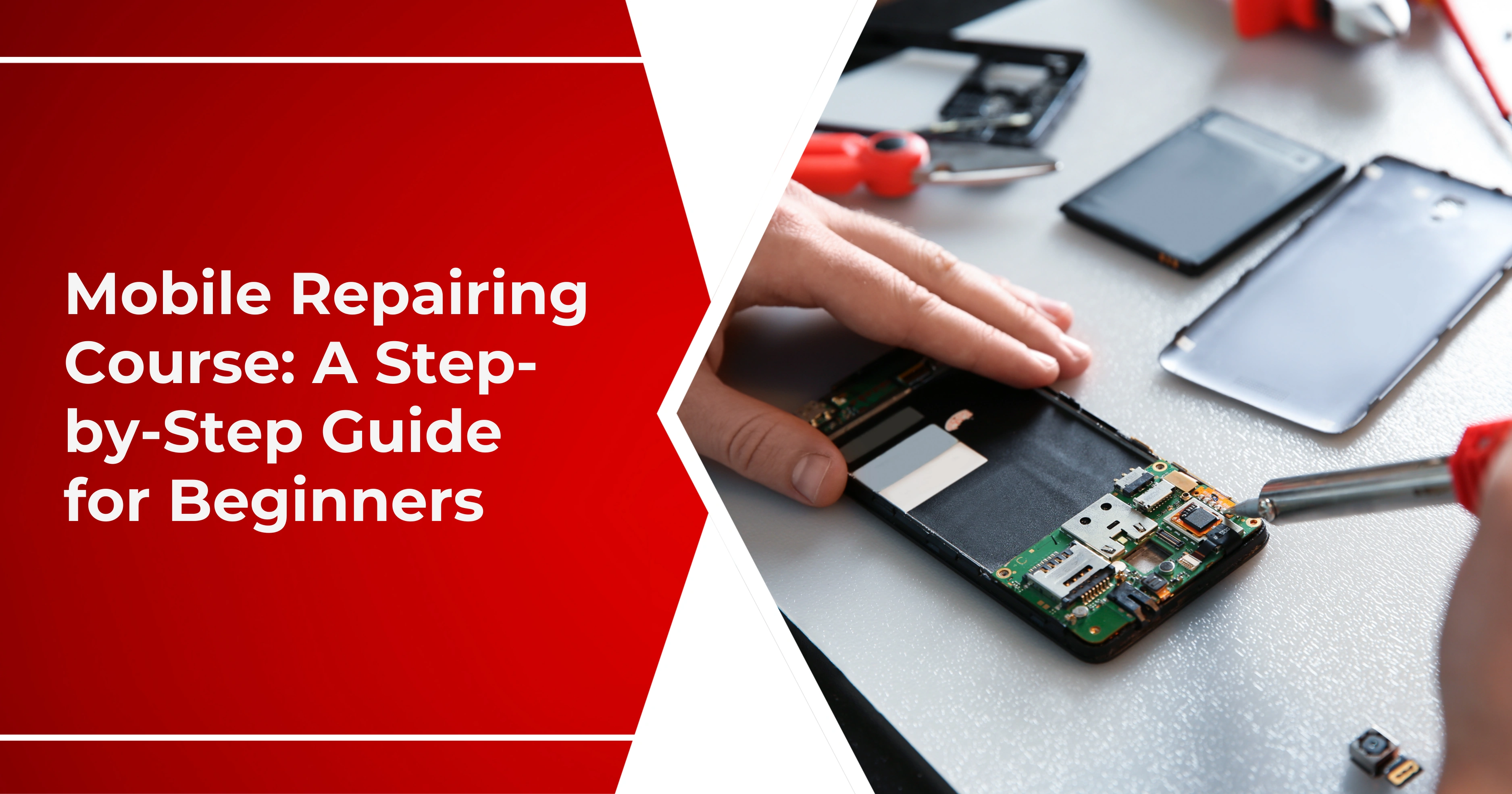
If you want to fix a mobile phone that is not charging, you need to know how to find the charging IC on the mobile board. Often, the issue is this small but crucial part in a phone: the charging IC. This is a chip that controls the way your phone receives power from the charger. If it gets damaged or doesn't work properly, the phone can refuse to charge.
This blog will teach you step-by-step how to identify a charging IC on any mobile PCB. You will also identify what tools you need and tips to find a Charging IC. If you're learning mobile repair or want to fix your phone at home, this blog is for you.
What is a Charging IC in a Mobile PCB?
- It allows for fixing a phone that is not charging at all.
- It serves quickly during the duration of mobile repair work.
- It improves your skills in mobile repair.
- It enables you to identify an exact faulty component and replace it.
Here is a very small chip built on the mobile phone's PCB (Printed Circuit Board), and hence very crucial. This chip controls whether power from the charger is going into the battery. If the charging IC is missing, the phone will not get charged.
The charging IC connects with other parts like resistors, capacitors, and connectors on the mobile PCB. If this IC gets damaged, the device will either fail to charge or charge at a slow rate and generate heat. Here are a few simple reasons why it matters to learn charging IC identification in the mobile PCB:
Tools You Need for Charging IC Testing
- Multimeter: To check the voltage on the IC and on other components.
- Magnifying Glass: A PCB magnifying glass or microscope allows for a clear view of small components.
- Soldering iron and hot air gun: to remove and fit the IC.
- DC Power Supply: It tests the power flow for the charging circuit.
- PCB Cleaner and Brush: Used to clean the board before testing.
Tools You Need for Charging IC Testing
These tools are essential for any mobile electronics troubleshooting guide. They help ensure accuracy and safety in your repairs.
Step-by-Step Guide to Identify Charging IC on Mobile Board
After preparing yourself, here is an easy method to carry out a charging IC ID on a mobile PCB.
Step 1: Power Off and Open the Phone
Ensure the phone is completely powered off. This helps prevent electrostatic shock. Go for the right screwdriver and tools to carefully open the phone. Once the back case is removed, one can gently draw out the PCB board. Be gentle, as you can easily damage its tiny, delicate parts if you apply undue pressure
Step 2: Locate the Charging Section on the PCB
The charging section is usually near the charging port on the PCB. This section has the USB connector, capacitors, resistors, and the charging IC. You identify it by tracing the path from where the charging socket starts. Having reference diagrams for that phone model is helpful if they are available.
Step 3: Visually Identify the Charging IC
Look for a black chip of medium size; its dimensions might be square or rectangular. Such chips are usually tagged with codes like U2, U4001, or other similar inscriptions. They are usually bigger than many nearby parts. Also, they might be close to the battery connector. Use a magnifier if you cannot see the codes with the naked eye.
Step 4: Refer to a Mobile Repair IC Diagram
If there's uncertainty, it is always handy to refer to a mobile repair IC diagram for the given phone model. These diagrams show how each component, such as the charging IC and the parts close to it, is laid out. They can help you find the exact location of the mobile charging IC. This is especially useful when using various models with different PCB layouts.
Step 5: Use a Multimeter to Test the Charging IC
Select the continuity setting on the meter to measure. Someone places the black probe on the ground, while the red probe touches every leg of the IC. If the multimeter continuously beeps for several legs, the IC could be shorted. This test can further confirm that the IC is damaged without removing it from the board.
Step 6: Understand Charging IC Symbol and Pinout
The charging ICs have their symbol and pin configuration set. These display the legs that connect to power, ground, battery, or USB. This helps in testing the correct pins. Sometimes, when there’s no voltage at the power input or output to the battery, a faulty IC might be the cause. Someone needs to replace it.
Step 7: Use Tools for Further Testing
You might also use a DC power supply and a thermal camera to inspect the charging section, as well as a multimeter. The DC supply applies controlled power to check if the heating up of the IC confirms its damage. These tools assure more reliable and precise testing.
Step 8: Check for Physical or Heat Damage
Sometimes, the charging IC may show physical signs of damage, like burns or cracks. In other cases, it may quickly become hot when someone supplies power. Examine the IC itself and the surrounding area with attention to detail.
Step 9: Remove and Replace the Charging IC
If you confirm the IC is faulty, remove it using a hot air gun. Clean the area with isopropyl alcohol. Then, put the new IC in the same spot. Solder the new IC well, taking care not to damage surrounding components. Test the phone again after the replacement. Check if the charging issue is fixed.
Step 10: Test the Phone After Repair
The moment you have replaced your charging IC, attach your battery and plug in your charger. You should see signs like the charging icon and a rise in battery percentage. Also, it shouldn’t get hot at all. If all goes well, you have just fixed it. If not, use a mobile PCB troubleshooting guide to check other nearby components.
Conclusion
Knowing about charging ICs in mobile PCBs is key for anyone learning mobile repair. If your phone won’t charge or you want to know about PCB components, this article has the basics you need. Using the right tools, like a multimeter, helps a lot.
Using a PCB troubleshooting guide and reading mobile repair IC diagrams can make diagnosing and fixing charging area issues easier. Never forget to make a note of charging IC failure symptoms to identify the fault in no time.
Replacing a charging IC can help you grow from a beginner to a pro. Keep practicing. Be patient. Treat every interaction with mobile PCBs carefully.
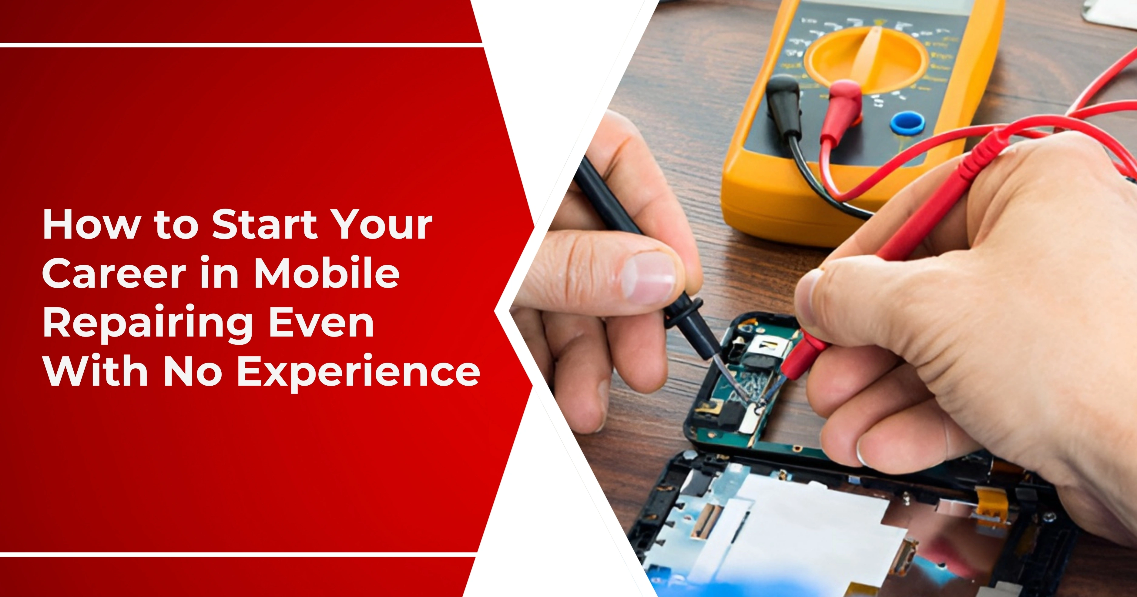
Start Your Career in Mobile Repairing Today!
Join India’s leading mobile repairing institute offering expert-led mobile repairing courses across major cities like Indore, Kolkata, Delhi, Patna, Agra, Karol Bagh, and Gurgaon. We provide hands-on practical training, access to certified faculty and advanced labs, and specialized courses in Patna. Plus, benefit from our 100% job placement support and start building your successful technical career today.
Enquire Now